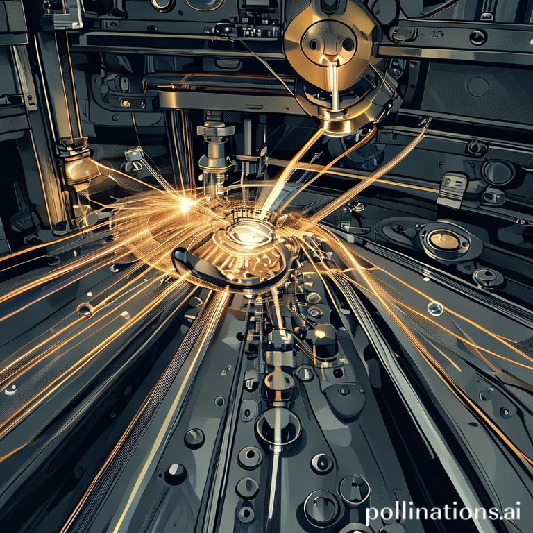
Have you ever wondered what makes your smartphone lightning-fast or powers the incredible AI tools we use daily? The answer lies in processor manufacturing. This microscopic world, indeed, drives a global “nanometer chase.” This relentless pursuit consequently creates smaller chips. They are also more powerful and energy-efficient. This further pushes technology’s boundaries. Ultimately, it’s a high-stakes game of innovation, massive investments, and significant geopolitical implications.
Imagine trying to build a city where every building is only a few atoms wide. Clearly, that’s the level of precision involved in modern processor manufacturing. This article therefore takes you deep inside this fascinating world. It also reveals cutting-edge technologies and monumental challenges. It further covers key players and geopolitical strategies. These subsequently shape our digital future.
The Drive for Miniaturization: Why Every Nanometer Matters
For decades, the semiconductor industry pursued a singular vision: cramming more transistors onto silicon chips. This ambition specifically began with Moore’s Law. Intel co-founder Gordon Moore observed it in 1965. He predicted that microchip transistors would double about every two years. This consequently meant more than packing components. It also promised an exponential surge in computing power and efficiency. This in turn transformed personal computers and global networks.
Some debate if Moore’s Law is slowing. Others question its physical limits. Yet, the drive for miniaturization remains undiminished. Shaving nanometers off transistor size indeed unlocks critical advantages. This thereby keeps processor manufacturing competitive.
Moore’s Law and the Perpetual Pursuit
The traditional interpretation of Moore’s Law envisioned a linear scaling down of individual transistor features. Today, the “law” instead increases transistor density. This further happens through various innovations, not just shrinking. This evolution thus ensures new chips deliver significant gains. Engineers meanwhile grapple with the atomic scale. The sheer ingenuity required to overcome these hurdles is therefore a testament to human innovation.
The Tangible Benefits of Tiny Transistors
Why is shrinking transistors so crucial for advanced processor manufacturing? Indeed, the benefits are profound. Moreover, they directly impact performance, efficiency, and design. This subsequently affects nearly every electronic device you use.
Here are the primary benefits driving the nanometer race:
- Increased Performance: Smaller transistors can switch between on and off states much faster. This consequently means higher clock speeds. Therefore, more instructions are processed per second. This is especially essential for demanding applications. These specifically include AI, HPC, and immersive gaming.
- Lower Power Consumption: Tiny transistors require less voltage to operate and dissipate less heat. This in turn extends battery life in mobile devices. It also reduces energy use in data centers. This is further vital for portability and sustainability.
- Compact Design: Higher transistor density allows chip designers to integrate more functionality into a single chip. This consequently leads to smaller, lighter devices. They further offer enhanced capabilities. Furthermore, power or features are not compromised. Indeed, imagine the powerful computers we carry in our pockets today, a direct result of this relentless miniaturization.

Extreme Ultraviolet Lithography (EUV): The Core Technology
Creating features smaller than a human hair on a silicon wafer seems like science fiction. Yet, it’s a daily reality in advanced processor manufacturing. This is largely thanks to revolutionary Extreme Ultraviolet (EUV) lithography. Without EUV, the nanometer chase would have stalled long ago.
EUV lithography uses highly energetic ultraviolet light with an incredibly short wavelength of 13.5 nanometers. This tiny wavelength therefore allows machines to carve intricate, microscopic patterns. They thus achieve unprecedented precision. This in turn enables features smaller than 7 nanometers. Traditional optical lithography, which relies on longer wavelengths, by contrast, simply cannot achieve this level of detail. It’s like trying to draw a fine line with a thick crayon versus a needle-point pen.
How EUV Works: A Glimpse into Atomic Precision
The EUV process is mind-bogglingly complex. It begins with a powerful laser striking molten tin droplets, creating a plasma that emits EUV light. This light is then precisely directed by near-perfect mirrors. These indeed are the flattest objects ever made by humans. It subsequently passes through a mask with the circuit design. Finally, it exposes a photoresist-coated silicon wafer. This entire process moreover occurs in a vacuum chamber. It specifically protects sensitive mirrors and wafers. Furthermore, even tiny dust particles are kept out. The required precision is therefore immense. It’s like shining a laser from Earth to hit a coin on the moon.

A detailed illustration of an EUV lithography machine, showing the complex optical path of the laser, the molten tin droplet generator, the series of perfectly reflective mirrors, the reticle (mask), and the silicon wafer being exposed. Annotations should explain each major component’s function in carving patterns for advanced processor manufacturing.
ASML: The Sole Gatekeeper of EUV Technology
One company stands alone at the apex of this technology: ASML from the Netherlands. ASML is indeed the sole producer of advanced EUV lithography machines. They are moreover essential for manufacturing cutting-edge chips. This unique position consequently gives ASML immense strategic importance. It is thus a critical choke point in the nanometer chase. This in turn affects the global semiconductor supply chain. Any disruption to ASML’s operations therefore would send shockwaves through the entire processor manufacturing industry.
The Hurdles on the Nanometer Path
Despite advancements, the nanometer chase faces formidable challenges. These specifically test engineering, physics, and economics. These hurdles consequently make advanced processor manufacturing an incredibly demanding field.
The Astronomical Price Tag of Innovation
Building and operating a modern “fab” is a colossal undertaking. It furthermore demands huge scale and expense. These facilities are in fact among the most complex and expensive industrial projects on Earth.
- Escalating Costs: A state-of-the-art fab costs over $20 billion to construct. It also requires specialized cleanrooms and advanced infrastructure. An army of skilled engineers is likewise needed. Individual EUV machines, the heart of advanced chip production, for example, exceed $150 million each. These costs are therefore a major barrier to entry. They thus concentrate advanced processor manufacturing in few hands.
- Complexity and Yield: The manufacturing process itself involves hundreds of intricate steps, each requiring extreme precision at the atomic level. Achieving high yields consequently becomes harder as features shrink. Yields are functional chips per wafer. Even a microscopic flaw moreover can render an entire chip useless, leading to significant material and time losses.

Battling Quantum Physics and Material Limits
Transistors approach just a few nanometers. This is a handful of atoms. Engineers consequently encounter fundamental physical limits. This is indeed where classical physics gives way to the strange rules of quantum mechanics.
- Quantum Effects: At these scales, phenomena like electron tunneling become significant. Electrons can “tunnel” through insulating barriers that should be impenetrable, leading to leakage currents. These unintended leaks consequently waste power and generate heat. This in turn affects the performance and efficiency of the chip.
- Material Constraints: Traditional silicon, the backbone of the semiconductor industry, is reaching its intrinsic limits. Researchers therefore explore new materials. They want to overcome these challenges. Finding a silicon replacement is moreover a monumental task. Enhancing silicon is also difficult.
The Environmental Footprint of Advanced Chip Production
The drive for ever-smaller chips also comes with a considerable environmental cost. The advanced tools and processes required for processor manufacturing are furthermore incredibly energy-intensive. EUV tools, for example, need much energy. They specifically require up to 10.2 GWh per tool annually. This ultimately equals thousands of homes’ annual electricity use.
This substantial energy demand consequently increases fabs’ carbon footprint. The industry therefore seeks sustainable manufacturing. It also pursues energy-efficient designs. It’s a critical balancing act between technological advancement and environmental responsibility.
The Global Arena: Key Players in Processor Manufacturing
Advanced processor manufacturing is not evenly distributed. Instead, a few titans dominate this concentrated field. These companies consequently wield immense technological and economic power, shaping the future of global computing.
Here’s a look at the major players and their contributions to the nanometer chase:
| Company | Headquarters | Key Advancements / Focus | Current / Upcoming Nodes | Global Market Share (Advanced Nodes) |
|---|---|---|---|---|
| TSMC | Taiwan | World’s largest independent foundry, leading edge in FinFET, developing advanced packaging. | Mass producing 7nm, 5nm. Developing 3nm, 2nm. | Over 90% of most advanced chips |
| Samsung | South Korea | Major foundry, pioneering Gate-All-Around (GAA) transistor technology. | Progress in 5nm, 3nm. Plans for 2nm (2025), 1.4nm (2027). | Significant contender |
| Intel | United States | Integrated Device Manufacturer (IDM), aiming to re-establish leadership, backside power delivery. | Currently 7nm equivalent (Intel 4). Aiming for 18A (~1.8nm) in H2 2025. | Rebuilding foundry services |
| ASML | Netherlands | Sole producer of Extreme Ultraviolet (EUV) lithography machines. | N/A (equipment supplier) | Monopoly on critical equipment |
| Rapidus | Japan | New consortium aiming for domestic 2nm chip production, leveraging IBM technology. | Aiming for pilot 2nm by 2025, mass production by 2027. | Emerging player |
TSMC: The Foundry Leader
TSMC (Taiwan Semiconductor Manufacturing Company): Taiwan’s TSMC is an undisputed leader. TSMC is indeed the world’s largest independent semiconductor foundry. It makes chips for most major tech companies. These companies design their chips but don’t produce them. TSMC mass-produced 7nm and 5nm chips. It also aggressively develops 3nm and 2nm processes. Taiwan thus produces over 90% of advanced processor chips. This further makes it a pivotal geopolitical player.
Samsung: A Major Contender
Samsung (South Korea): Another formidable contender, Samsung, has made significant strides in both 5nm and 3nm nodes. Samsung specifically pushes Gate-All-Around (GAA) transistor technology. This is moreover crucial for smaller nodes. It plans 2nm chips by 2025 and 1.4nm by 2027. Samsung’s dual role as both a memory producer and a foundry consequently positions it uniquely in the industry.
Intel: Re-establishing Leadership
Intel (United States): Intel pioneered processor manufacturing. It faced recent challenges. Now, it vigorously works to re-establish leadership. Intel plans for its 18A process by H2 2025. To clarify, this is roughly 1.8nm. Intel therefore invests heavily to regain its top position. The company’s strategy furthermore involves internal manufacturing and also offering foundry services to external clients.
Geopolitical Stakes: The Race for Chip Sovereignty
Beyond the technological marvels and economic investments, the nanometer chase has profound geopolitical implications. Semiconductors are not just components. They are in fact strategic assets. They are moreover vital for national security, economic competitiveness, and independence.

National Security and Economic Imperatives
The reliance of modern economies and defense systems on advanced chips cannot be overstated. Semiconductors power AI and 5G networks. They also guide advanced military systems. They further form the bedrock of the digital age. Designing and manufacturing these chips is therefore crucial. It moreover measures a nation’s strength and resilience.
COVID-19 exposed supply chain vulnerabilities. This consequently intensified the race for semiconductor self-sufficiency. Nations realized over-reliance was risky. Relying on one region for components indeed caused vulnerability. This further meant economic disruption or national security risks.
Government Initiatives Driving Domestic Production
In response to these concerns, governments worldwide are pouring billions into domestic processor manufacturing capabilities. Moreover, they aim to lessen reliance on Asian supply networks. Taiwan currently holds a disproportionate share. This consequently affects advanced chip production.
United States: The CHIPS and Science Act
- United States: The U.S. CHIPS and Science Act is a landmark initiative. It specifically dedicates over $52 billion. This further boosts domestic semiconductor research, development, and manufacturing. The goal is ultimately to onshore critical production and secure future technological leadership.
European Union: The EU Chips Act
- European Union: The EU Chips Act aims to mobilize over €43 billion. This furthermore includes public and private investment. Europe thus seeks to double its global chip production share to 20% by 2030.
China’s Drive for Self-Sufficiency
- China: China prioritizes semiconductor self-sufficiency. It consequently invests heavily in its domestic chip industry. National plans and subsidies therefore reduce foreign technology dependence.
Japan: Rapidus and 2nm Ambitions
- Japan: Japan’s Rapidus initiative is making a concerted effort. It aims to re-enter advanced processor manufacturing. Rapidus specifically collaborates with IBM. It aims for a 2nm pilot line by 2025. Mass production should then begin by 2027. It also leverages expertise in materials and equipment.
The stakes are enormous. Control over advanced processor manufacturing is indeed key. It consequently provides a significant advantage in the global tech arms race. The semiconductor industry furthermore impacts the U.S. economy. This specifically includes microelectronics. Its value was $268B to $297B in 2022. The global memory market will exceed $190 billion in 2025. High-bandwidth memory (HBM) primarily fuels this. The insatiable demands of AI also drive it.
Beyond the Nanometer: The Future of Processor Manufacturing
Traditional linear scaling approaches physical limits. Processor manufacturing therefore explores new avenues. This in turn advances computing power. The future isn’t just about shrinking; it’s instead about innovating in three dimensions and embracing entirely new paradigms.
Next-Gen Transistors and Packaging Innovations
The industry consequently develops sophisticated transistor architectures. It also uses advanced packaging techniques. These ultimately overcome limits and deliver next-gen performance.
- Advanced Transistor Architectures:
Gate-All-Around (GAA) Transistors: These innovative designs replace FinFET structures. A gate consequently surrounds the channel on all four sides. This therefore provides superior electrostatic control. It also reduces leakage currents. Performance likewise improves at small scales. Both Samsung and Intel are thus* heavily investing in GAA.
Nanosheet Transistors: Nanosheet transistors are a GAA variation. They specifically use horizontal silicon layers for the channel. This consequently* allows greater design flexibility and performance tuning.
- 3D Integration and Advanced Packaging:
Chip Stacking: Rather than shrinking transistors horizontally, engineers are now stacking multiple layers of transistors vertically. This “3D integration” consequently increases transistor density. It further does not require shrinking individual transistors. It also* offers significant performance and power efficiency.
Heterogeneous Integration: This combines different processors and accelerators. CPU, GPU, memory, and AI accelerators are integrated. They form a single package. This approach consequently optimizes performance for specific workloads. It also extends gains beyond monolithic chips. Intel’s backside power delivery is for example an example. It routes power from the chip’s back to transistors. This subsequently* frees front space for data routing.


Exploring New Horizons: Materials and Computing Paradigms
Researchers look beyond silicon technology. They therefore investigate new materials. They also explore different ways of computing.
- New Materials: The search for alternatives to silicon is intense. Research consequently explores new materials. These specifically include graphene and carbon nanotubes. They aim to overcome silicon’s limitations. This further could enable faster, more energy-efficient transistors. They might also have novel properties.
- New Computing Paradigms: The long-term future may lie beyond traditional silicon-based architectures. Alternative computing methods being explored therefore include:
* Quantum Computing: Harnessing quantum mechanical phenomena (superposition, entanglement) to solve complex problems intractable for classical computers.
Neuromorphic Computing: This designs chips mimicking the human brain. It consequently* offers incredible potential for AI and machine learning.
Moore’s Law interpretation may evolve. Still, innovation in processor manufacturing remains vibrant. The nanometer chase thus drives the industry. It consequently blends scientific discovery and engineering ingenuity. Economic ambition and geopolitical maneuvering are also key. It moves toward unprecedented computing power. This ultimately shapes our current digital world and the future.
What is the biggest breakthrough in processor manufacturing? What impact will it have on our daily lives? Share your thoughts in the comments below!


