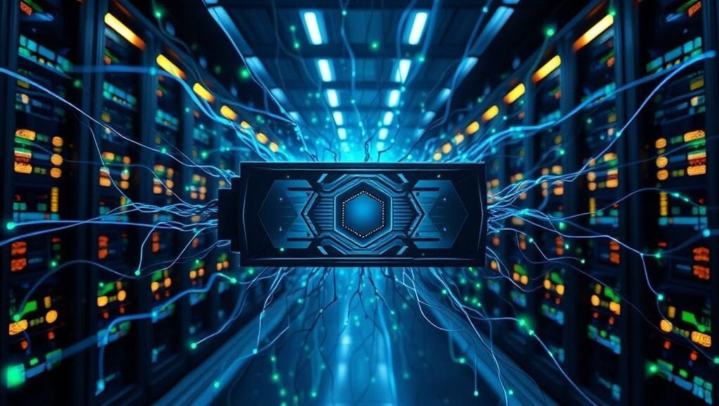
The AI field rapidly evolves, demanding immense computational power. Therefore, understanding Blackwell architecture performance gains is crucial for future progress. Large language models and scientific discovery push processing, memory, and communication limits. NVIDIA, a leader in accelerated computing, specifically engineered its Blackwell architecture to meet these demands. They unveiled it in March 2024, naming it after mathematician David Blackwell. This innovative design fundamentally redesigns GPU technology. Consequently, it delivers substantial performance improvements, unparalleled efficiency, and unprecedented scalability. Ultimately, Blackwell will power tomorrow’s “AI factories“.

The Dawn of a New AI Era: Unpacking Blackwell Architecture Performance Gains
Artificial intelligence has indeed evolved remarkably rapidly, driving immense demand for generative AI computing. Models like ChatGPT have captivated the public and sparked innovation. Yet, training these colossal models, often comprising trillions of parameters, necessitates vast computational power. Real-time inference, using these trained models to generate outputs, demands exceptional speed and efficiency. Although the Hopper architecture was groundbreaking, it faced limitations as model sizes grew exponentially. As a crucial Hopper successor, the need for faster training, quicker inference, and superior power efficiency became critically important for continued AI performance advancements.
NVIDIA recognized this growing gap, meticulously designing NVIDIA Blackwell from the ground up to address these emerging issues. This architecture is not merely optimized for today’s AI; it’s robustly built for the AI landscape of the next decade, ensuring unmatched performance. Its core idea centers on overcoming the physical and technical limits inherent in single-chip designs, meticulously optimizing every part of the AI compute pipeline. The overarching goal is clear: to efficiently train and infer even the most complex AI models, including those with up to 10 trillion parameters. It promises unprecedented speed and cost-effectiveness. The anticipated advancements represent generational leaps that will fundamentally reshape what is possible in artificial intelligence.
Core Architectural Innovations: Unlocking Significant Blackwell Architecture Performance Gains
The architecture undeniably delivers impressive performance improvements. These substantial architectural enhancements stem from a sophisticated combination of breakthrough technologies, rather than just one singular advancement. Indeed, every architectural component has been meticulously engineered, consequently pushing the frontiers of generative AI computing to entirely new limits.
Blackwell’s key physical innovation, moreover, is its multi-die “superchip” design. Unlike traditional GPUs, which are inherently limited by single-wafer manufacturing processes, NVIDIA Blackwell strategically unites two massive GPU dies. Fabricated using a custom TSMC 4NP process, this innovative approach significantly boosts capabilities. The flagship B200 GPU, for example, exemplifies this, packing an astounding 208 billion transistors—over 2.5 times more than the previous Hopper GH100.

Crucially, these two dies function seamlessly as a single, unified GPU. They connect flawlessly via a high-speed, 10 TB/s chip-to-chip interface. This innovative method, consequently, allows NVIDIA to achieve more on-chip resources, reaching a level previously impossible with a monolithic die. Ultimately, this foundational design provides a massive boost to overall capabilities, driving superior AI performance across the board.
Advanced AI Computation: Driving Blackwell Speedups
Modern large language models heavily rely on the Transformer architecture; consequently, the architecture was specifically optimized to accelerate it. The new second-generation Transformer Engine introduces sophisticated micro-tensor scaling and advanced dynamic range management. This, in turn, enables support for 4-bit floating-point (FP4) AI operations, a cutting-edge advancement contributing significantly to Blackwell speedups.
FP4 precision, indeed, dramatically reduces both memory and computational overhead for AI calculations. Integrating seamlessly into frameworks like NVIDIA TensorRT-LLM and NeMo, this innovation offers dual benefits for AI performance. It can, first, double compute performance for inference tasks and, second, support model sizes twice as large, all while diligently maintaining high accuracy.
This capability is vital for deploying vast LLMs, which often face bottlenecks in memory capacity and inference speed. Furthermore, alongside FP4, NVIDIA Blackwell enhances support for FP8. Leveraging these lower precision formats effectively, therefore, drives significant advancements in both speed and efficiency for generative AI computing.

Scaling and Data Pipeline Innovations Boosting NVIDIA Blackwell’s AI Performance
Rapid and efficient GPU communication is absolutely vital in large AI training clusters. To achieve this, NVIDIA introduces NVIDIA’s fifth-generation NVLink interconnect technology. This upgraded system, for instance, delivers an astonishing 1.8 TB/s of bidirectional bandwidth per GPU, representing a substantial increase over prior generations and contributing to significant AI performance boosts. Furthermore, the NVSwitch facilitates this high-speed link, allowing seamless communication across an unprecedented number of GPUs.
NVLink, indeed, enables a single Blackwell cluster to utilize up to 576 GPUs, operating them effectively as one massive, unified computational engine. For example, a 72-GPU NVL72 pod functions entirely as a single unit. It provides a staggering 1.4 exaFLOPs of AI compute and, moreover, pools an enormous 30 TB of shared memory. This advanced connectivity is, therefore, crucial for efficiently training the largest, most complex AI models, ensuring data moves between GPUs with minimal latency and amplifying overall system capabilities at scale.

Optimized Memory and Accelerated Data Flow: Contributing to NVIDIA Blackwell’s AI Performance
Large AI models inherently demand vast amounts of high-bandwidth memory (HBM) for parameters and activations. Blackwell GPUs, such as the B200, meet this formidable challenge with 192 GB of HBM3e memory. This is, notably, over double the effective VRAM of the previous Hopper H100, a clear differentiator for this Hopper successor. Furthermore, this impressive capacity comes with an aggregate memory bandwidth of 8 TB/s. This combination directly resolves a critical bottleneck in large AI models, which often struggle with memory and bandwidth limitations. Ultimately, more memory allows larger models on fewer GPUs, and higher bandwidth speeds data access, consequently leading to significant AI performance boosts for the platform in training and inference.

AI workloads, moreover, involve substantial data loading and preprocessing, not solely raw computation. The architecture, therefore, addresses this often-overlooked area with a new on-die decompression engine. This specialized hardware dramatically accelerates data loading and analytics, reportedly processing data up to 800 GB/s. This improvement, consequently, makes it six times faster than Hopper for large datasets. As a result, GPUs dedicate more time to AI computations and less time waiting for data. Ultimately, this enhances overall system efficiency and significantly boosts the architecture’s capabilities.
Assessing Blackwell’s Innovation: Evaluating B200 GPU AI Performance: Maximizing Blackwell Architecture Performance Gains
For enterprise deployments, security is absolutely paramount. The platform, in fact, sets a new standard as the first GPU to support TEE-I/O, enabling end-to-end encryption of data even while in use. Furthermore, advanced confidential computing features are intricately integrated. These capabilities, together, ensure highly secure AI performance operations with virtually no performance compromise. This, consequently, represents a significant advantage for handling sensitive data and operating within regulated industries, bolstering its overall effectiveness in demanding environments.
Beyond security, a dedicated RAS Engine ensures intelligent resiliency and maximizes uptime. This engine, moreover, employs AI-driven predictive management to anticipate and proactively mitigate potential hardware issues. It also reliably guarantees consistent, dependable AI performance. Thus, these combined features firmly establish this platform as a robust and trustworthy platform, capable of supporting the most demanding AI applications with assured operational integrity.
Quantifying the Leap: Substantial Blackwell Architecture Performance Gains
Blackwell architecture offers truly remarkable performance upgrades when compared to its predecessor, Hopper H100/H200. Indeed, these architectural innovations directly translate into significant enhancements across various benchmarks. Overall, the platform performs up to 2.5 times faster than Hopper, which signals a fundamental shift in computational capability and demonstrates substantial improvements.
For computationally intensive AI training, Blackwell offers substantial increases in speed. In fact, it often achieves 3 to 4 times faster speeds. This acceleration greatly benefits AI researchers, as they can iterate on models more quickly, thereby shortening development cycles and enabling more complex architectures for advanced AI tasks. Furthermore, the architecture truly excels in AI inference, providing staggering improvements. Users can expect up to 15 times faster inference for many large models; specifically, it is up to 30 times faster for general computational workloads. This dramatically reduces latency, making real-time applications practical for widespread deployment. Moreover, the new FP4 precision is a key driver for these impressive gains.
Blackwell’s raw compute throughput intrinsically underpins these performance leaps. The B200 GPU, for example, offers about 2.3 times the throughput of the H100. This applies consistently at FP16/BF16 and FP8 precision levels. Furthermore, the new FP4 mode provides an additional 2x boost, coming on top of the already significant gain. This exponential increase in compute throughput, therefore, forms the bedrock for all other performance metrics, thus solidifying its monumental advancements in computational power.

Assessing Blackwell’s Innovation and the Blackwell Architecture Performance Gains
Beyond raw speed, the new architecture also introduces unprecedented power efficiency, which directly translates to significant cost savings and a reduced environmental footprint. For large language model (LLM) inference, Blackwell is remarkably power-efficient, achieving up to 25 times less cost and energy compared to Hopper. Therefore, this efficiency is absolutely critical for scaling generative AI computing infrastructure sustainably, further emphasizing the widespread benefits of the new platform.
Consider NVIDIA CEO Jensen Huang’s vivid example. Training a GPT-4 sized AI model once needed 8,000 Hopper H100 chips and consumed 15 megawatts of power. With Blackwell, however, the same task now uses only 2,000 B200 GPU chips, requiring a mere four megawatts. This represents a substantial 75% reduction in power consumption and also reduces the chip count for the same workload. This powerfully shows the platform’s massive efficiency gains. In short, Blackwell truly serves as the foundational engine for future “AI factories.”

Addressing Modern AI Challenges with Superior Blackwell Architecture Performance Gains
NVIDIA’s Blackwell architecture has generated immense enthusiasm and even astonishment across the tech industry. Analysts, for example, laud the platform, calling it “the most ambitious project in Silicon Valley.” Furthermore, they note how it “shocked the market.” This widespread sentiment, consequently, highlights its significant leap forward in generative AI computing.
Blackwell is, undeniably, a decisive move that reinforces NVIDIA’s dominant position in the AI chip market. In fact, experts predict it will be a potent catalyst for a new growth phase, driven by the profound advancements in its design. Demand for these cutting-edge GPUs, for instance, is expected to far outpace supply in the initial years. Moreover, NVIDIA CEO Jensen Huang described Blackwell’s demand as “insane,” which emphasizes its critical importance.
Huang aptly calls Blackwell “the engine to power this new industrial revolution,” thereby highlighting its fundamental importance to the global AI ecosystem. Major cloud providers, such as Amazon Web Services, Google Cloud, Microsoft Azure, and Oracle Cloud Infrastructure, are making substantial commitments. Leading AI companies are also doing so. This rapid adoption, therefore, signals profound industry confidence in the platform’s capabilities and its promise of superior computational performance.
Assessing Blackwell’s Innovation
Some analysts, however, offer a more tempered assessment. One analyst, for example, called the Blackwell chip “a repackaging exercise.” This view suggests the platform simply delivers more compute, faster, all within the same power and space budget. However, its core architectural innovations might appear evolutionary rather than revolutionary conceptual breakthroughs. Even this measured view, nevertheless, concedes an important point: NVIDIA’s aggressive, first-to-market strategy strengthens its image as a relentless innovator. It further drives demand and consistently maintains market leadership for generative AI computing. Regardless of interpretation, consensus confirms its advancements are real, substantial, and, moreover, vital for advancing AI.
Addressing the Challenges of Modern AI
NVIDIA Blackwell directly addresses the multifaceted challenges that confront modern AI development and deployment. Notably, the exponential growth of LLMs and generative AI computing has pushed existing hardware to its limits, thus creating bottlenecks in several key areas:
- Compute Bottleneck: Training models with trillions of parameters demands unimaginable raw compute power. However, Blackwell’s multi-die design and advanced Transformer Engine directly tackle this, offering unprecedented FLOPs and boosting AI performance.
- Memory Bottleneck: Storing and accessing vast model parameters requires immense HBM capacity and bandwidth. Yet, Blackwell’s 192GB HBM3e and 8 TB/s bandwidth alleviate this constraint, enabling larger models to reside on-chip.
- Communication Bottleneck: In large-scale training clusters, slow inter-GPU communication can significantly hamper AI performance. Conversely, the 1.8 TB/s NVLink ensures that GPUs act as a cohesive unit, consequently eliminating communication as a limiting factor and contributing to Blackwell speedups.
- Efficiency Bottleneck: The sheer power consumption of AI factories is a growing concern. However, Blackwell’s 25x improvement in power efficiency for inference is a game-changer, improving sustainability and lowering operational costs, thereby enhancing its overall efficiency.
- Data Pipeline Bottleneck: Getting data to the GPUs fast enough is often overlooked. Thus, the dedicated decompression engine ensures that data ingestion keeps pace with compute, thereby maximizing GPU utilization and boosting overall AI performance for NVIDIA Blackwell.
Blackwell systematically addresses these bottlenecks. It does not just offer mere performance improvements; instead, it fundamentally redefines AI’s operational parameters. This, consequently, enables researchers and businesses to tackle previously intractable problems, propelled by its superior capabilities.
The Blackwell Ecosystem: More Than Just Hardware
NVIDIA Blackwell is not merely a chip; rather, it is the core of an entire ecosystem. NVIDIA employs a holistic approach, which integrates the powerful hardware with a robust software stack. Such a stack includes CUDA, TensorRT-LLM, NeMo, and various AI frameworks and libraries. As a result, developers can fully leverage these architectural innovations without needing to re-engineer their entire software. The synergy between hardware and software is a hallmark of NVIDIA’s strategy. Indeed, it is crucial for realizing the full potential of these advancements in real-world applications. This complete platform approach, moreover, accelerates adoption and ensures the platform’s power is readily accessible to the broader AI community for generative AI computing and all forms of accelerated computing.
Conclusion
NVIDIA’s Blackwell architecture marks a seismic shift in AI performance capabilities. It combines several potent features. These include its multi-die “superchip” design, the efficient second-generation Transformer Engine with FP4 precision, and hyper-scale connectivity from its fifth-generation NVLink. Significantly increased HBM3e memory is also present. Together, these elements deliver truly substantial advancements. These innovations, therefore, bring unparalleled gains in AI training and inference speeds. They also offer remarkable energy efficiency and robust security features, making NVIDIA Blackwell a game-changer.
As the world moves towards an AI-driven future, demands on computational infrastructure will only intensify. The architecture is not just meeting these demands; instead, it is defining a new frontier. Indeed, it stands as a critical enabler for the next generation of AI and generative AI computing. It empowers researchers, developers, and businesses to build, train, and deploy AI models of unprecedented scale and sophistication. The profound improvements will undoubtedly accelerate the “new industrial revolution” NVIDIA envisions, thereby shaping AI’s capabilities and accessibility for years to come.
Frequently Asked Questions
NVIDIA Blackwell significantly leaps over Hopper in AI performance and efficiency. As a true Hopper successor, it delivers up to 2.5 times faster overall performance. AI training is accelerated up to four times, and AI inference boosts up to 30 times for specific workloads. Blackwell also offers up to 25 times better power efficiency for LLM inference. It notably features 192 GB of HBM3e memory, compared to Hopper’s 80 GB HBM3, showcasing the advancements of the B200 GPU.
Blackwell’s FP4 (4-bit floating-point) precision dramatically enhances AI performance efficiency. This innovation is intricately integrated into the second-generation Transformer Engine. It reduces memory usage and computational overhead. Consequently, it can double compute performance and supports AI models twice as large for inference tasks, all while maintaining crucial accuracy. This capability, moreover, is vital for powering very large language models and achieving significant Blackwell speedups.
NVLink is NVIDIA’s high-speed interconnect technology. It is central to NVIDIA Blackwell’s power. The fifth-generation NVLink in the architecture, for instance, offers an impressive 1.8 TB/s of bidirectional bandwidth per GPU. This massive bandwidth, therefore, lets hundreds of GPUs communicate seamlessly. Up to 576 GPUs can connect. As a result, they operate as a single, unified computational engine. This is essential for training enormous AI models across vast clusters with minimal latency, driving immense advancements in processing power.
Blackwell’s Market Impact and Deployment
The new architecture’s capabilities will primarily benefit industries that heavily rely on large-scale AI and generative AI computing. This includes major cloud computing providers and advanced AI research laboratories. Furthermore, sectors like pharmaceuticals, used for drug discovery, stand to gain. Financial services, for complex modeling, will also benefit significantly. The automotive industry, especially for autonomous driving, will see clear advantages. Also, any sector developing or deploying advanced generative AI and large language models will experience substantial benefits from NVIDIA Blackwell.
NVIDIA unveiled Blackwell GPUs in March 2024. However, they are specifically engineered for data centers and AI factories, not for individual consumers. Major cloud providers and leading AI companies are rapidly adopting this architecture. Consequently, general availability for large-scale enterprise deployments likely started in late 2024 and is also expected by early 2025 for the B200 GPU and other NVIDIA Blackwell products.


